iTranslated by AI
Simple Electronic Kokkuri-san


Kokkuri-san
Kokkuri-san is a well-known divination ritual. It is performed using the following steps:
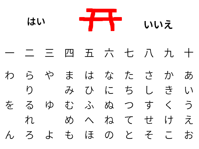
Kokkuri-san Paper
- Prepare a piece of paper and a coin as shown in the figure above. Place the coin on the paper and rest your index finger on the coin.
- Call out, "Kokkuri-san, please come." At this point, the coin may move, which is attributed to Kokkuri-san.
- Ask Kokkuri-san several questions. Kokkuri-san will answer by moving the coin.
- Once you are finished with Kokkuri-san, you must release him. Call out, "Kokkuri-san, please return home."
- That is all.
Simplified Kokkuri-san through Electronics
Among the behaviors of Kokkuri-san mentioned above, we will build a version that can answer "yes" or "no" questions using electronics. This project will not use a microcontroller.
Overall Circuit Diagram
The overall circuit diagram is shown below. The IC used is a 74HC14 compatible part. The power supply is assumed to be 3V from two AA batteries.

Circuit diagram for the simplified Kokkuri-san
Explanation of Each Part
IC 74HC14
The 74HC14 is a CMOS Schmitt-trigger inverter.
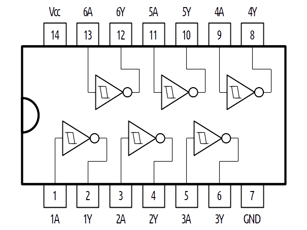
Pin connection diagram
What is an Inverter?
An inverter is a component that inverts logic. In other words, when a high level (3 V) is input, it outputs a low level (0 V), and when a low level is input, it outputs a high level.
What is a Schmitt Trigger?
A circuit with hysteresis characteristics in its input—where the threshold for switching from a high level to a low level differs from the threshold for switching from a low level to a high level—is called a Schmitt trigger.
Oscillation Circuit
The oscillation circuit is located around the bottom left of the circuit diagram.

Oscillation circuit
Explanation
You can verify the sequence of operations described here in the simulator.
-
Assume that the voltage across
C C R -
As charging progresses and the inverter's input voltage exceeds the threshold, the output switches to a low level. Then,
C R -
As discharging progresses and the inverter's input voltage crosses the threshold, the output switches back to a high level. Thereafter, this operation is repeated.
Oscillation Frequency Guidelines
The approximate oscillation frequency
Sample-and-Hold Circuit
The sample-and-hold circuit is located around the bottom center of the circuit diagram.
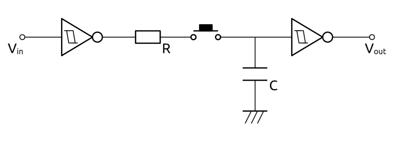
Sample-and-hold circuit
Explanation
You can verify the sequence of operations described here in the simulator.
-
When the switch is not pressed, the output of the first-stage inverter does not reach the next-stage inverter.
-
When the switch is pressed,
C -
When the switch is released, the input to the next-stage inverter becomes the voltage stored in
C C -
As long as the switch remains released, the input level of the next-stage inverter does not change, so the
V_{out}
Caution
When connecting a large capacitor (>500 pF) to the output terminal of a CMOS IC, a large current may flow at the moment of signal switching, which can cause noise or damage the IC. To prevent this, a current-limiting resistor is connected (
Note that this
LED Drive Circuit
The right side of the circuit diagram is the circuit that drives the LEDs.
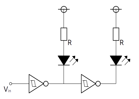
LED drive circuit
Explanation
When
Resistor Values
Resistor
Power Supply Circuit
The top center of the circuit diagram is the power supply circuit. The power source consists of two AA batteries connected in series.
About Capacitors
Operation Check
When you release the switch, only one of the left or right LEDs will light up randomly. While the switch is being pressed, the LEDs blink at high speed.
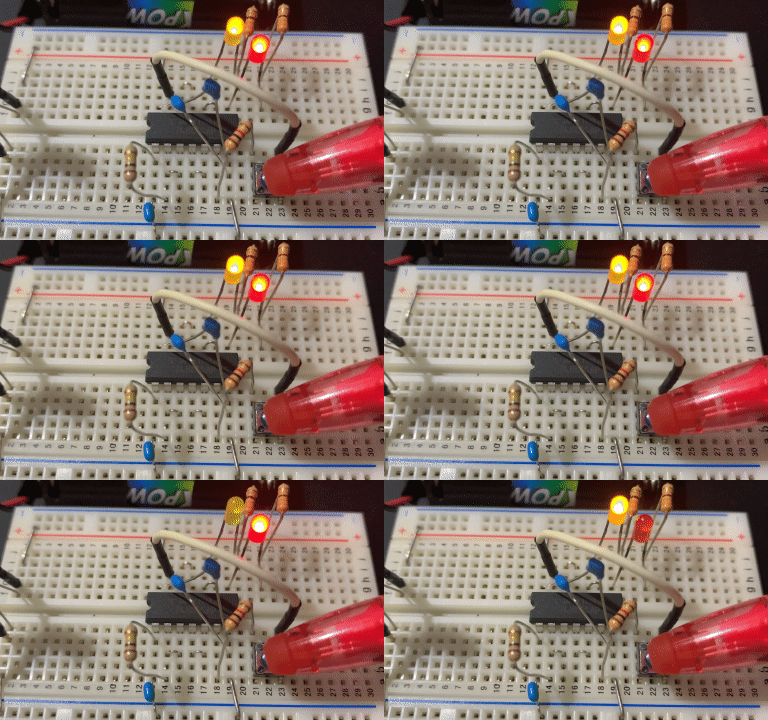
Leaving the decision to Kokkuri-san
Conclusion
That's all.
There was not a single element of programming in this article. Since Zenn is an "information-sharing community for engineers," I thought it would be nice if there were a world where people specializing in the design and production of electronic circuits could share their expertise, or mechanics could share tips for using a lathe.
References
-
Hiroshi Tanigawa. Explanation of "Schmitt Trigger Circuit". Synapse Hard Production Records. 2019-12-02. (accessed 2022-07-18).
-
bbradio. Oscillation Circuit Using a Schmitt Inverter. Breadboard Radio. 2008-04-21. (accessed 2022-07-18).
-
Toshiba Electronic Devices & Storage Corporation. Connecting Load Capacitance to CMOS Output Terminals. Precautions for Using CMOS Logic ICs. (accessed 2022-07-18).
Discussion